

 |
Lithography Etching Coating and Bonding for Customized Piezoelectric Wafers
Product Details:
| Place of Origin: | China |
| Brand Name: | CQTGROUP |
| Certification: | ISO:9001, ISO:14001 |
| Model Number: | Chip Foundry Services |
Payment & Shipping Terms:
| Minimum Order Quantity: | 1 pcs |
|---|---|
| Price: | Negotiable |
| Packaging Details: | Cassette/ Jar package, vaccum sealed |
| Delivery Time: | 1-4 weeks |
| Payment Terms: | T/T |
| Supply Ability: | 10000 pcs/Month |
|
Detail Information |
|||
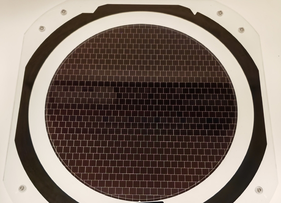
| Product: | Chip Foundry Services | Wafer Materials: | LiNbO₃,LiTaO₃,Crystal Quartz,Glass,Sapphire Etc. |
|---|---|---|---|
| Type Of Service: | Lithography,Etching,Coating, Bonding | Lithography: | EBL Proximity Lithograph OStepper Lithography |
| Etching: | IBE,DRIE,RIE | Bonding:: | Anodic,Eutectic,Adhesive,Wire Bonding |
Product Description
State of the Art Lithography Etching Coating and Bonding for Custom Piezoelectric Wafers
We specialize in providing comprehensive chip foundry services, catering to clients who require high-quality wafer processing and fabrication. By simply providing design schematics and specifications, we deliver tailored solutions that meet your exact needs. Our extensive range of wafers includes Lithium Niobate (LiNbO₃), Lithium Tantalate (LiTaO₃), Single Crystal Quartz, Fused Silica Glass, Borosilicate Glass (BF33), Soda-Lime Glass, Silicon Wafers, and Sapphire, ensuring versatility for diverse applications.
Our proven track record includes successful projects such as Surface Acoustic Wave (SAW) Interdigital Transducers, Lithium Niobate Ring Transducers, Microfluidic Chips, and various MEMS designs.
Advanced Processing Capabilities
- Lithography:
- Electron Beam Lithography (EBL)
- Proximity Lithography
- Stepper Lithography
- Etching:
- Ion Beam Etching (IBE)
- Deep Reactive Ion Etching (DRIE)
- Reactive Ion Etching (RIE)
- Coating:
- Electron Beam Evaporation
- Magnetron Sputtering
- Low-Pressure Chemical Vapor Deposition (LPCVD)
- Plasma-Enhanced Chemical Vapor Deposition (PECVD)
- Atomic Layer Deposition (ALD)
- Bonding:
- Anodic Bonding
- Eutectic Bonding
- Adhesive Bonding
- Wire Bonding
- Thinning, Cutting, and Drilling:
- Precision Grinding and Thinning
- Dicing and Cutting
- Laser Drilling
State-of-the-Art Equipment
Our facility is equipped with advanced supporting machinery, including Grinding Machines, Thinning Machines, Polishing Machines, and Dicing Saws, ensuring the highest standards of precision and efficiency throughout the fabrication process.
Whether you are developing cutting-edge MEMS devices, microfluidic systems, or specialized transducers, our team is committed to delivering exceptional quality, reliability, and technical support. Partner with us to bring your innovative designs to life with unmatched expertise and state-of-the-art capabilities.