

 |
High-Performance MgO Wafers For Advanced Electronic And Photonic Applications
Product Details:
| Place of Origin: | China |
| Brand Name: | CSIMC |
| Certification: | ISO:9001, ISO:14001 |
| Model Number: | MgO wafer |
Payment & Shipping Terms:
| Minimum Order Quantity: | 10pcs |
|---|---|
| Price: | Negotiable |
| Packaging Details: | Cassette/ Jar package, vaccum sealed |
| Delivery Time: | 1-4 weeks |
| Payment Terms: | T/T |
| Supply Ability: | 10000 pcs/Month |
|
Detail Information |
|||
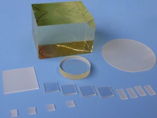
| Materials: | MgO Wafer | Size: | 10x10,15x15,20x15,20x20mm |
|---|---|---|---|
| Thickness: | 0.5mm,1.0mm | Surface Finish: | DSP SSP |
| Orientation: | <001>±0.5º | Purity: | 99.95% |
| Highlight: | Photonic Applications MgO Wafers,High Performance MgO Wafers,Advanced Electronic MgO Wafers |
||
Product Description
Choose Our High-Performance MgO Wafers for Advanced Electronic and Photonic Applications and Stay Ahead of the Competition
Elevate your research and development with the MgO Single Crystal Substrate, a premium material known for its exceptional electrical, optical, and mechanical properties. Ideal for a wide range of applications, MgO Single Crystal Substrate offers high crystal quality, low lattice mismatch, and excellent thermal stability.
Our MgO Single Crystal Substrate is meticulously grown and polished to meet the highest standards of purity and uniformity. Its superior crystalline structure ensures minimal scattering and absorption, making it an ideal choice for high-performance electronic devices, optical components, and thin-film coatings.
Discover the benefits of MgO Single Crystal Substrate for your next project. With its unmatched performance and reliability, MgO Single Crystal Substrate is the perfect foundation for your cutting-edge research and development. Contact us today to learn more about our MgO Single Crystal Substrate and how it can enhance your applications. With our commitment to quality and innovation, you can trust that our MgO Single Crystal Substrate will meet and exceed your expectations.
![]()
| Main performance parameters | |
| Growth method | arc melting method |
| Crystal structure | cube |
| Lattice constant | a=4.130 Å |
| Melting point (℃) | 2800 |
| purity | 99.95% |
| Density (g/cm3) | 3.58 |
| hardness | 5.5(mohs) |
| Coefficient of thermal expansion (/℃) | 11.2x10⁻⁶ |
| Crystal cleavage plane | <100> |
| Optical transmission | >90%(200~400nm),>98%(500~1000nm) |
| Dielectric constant | ε= 9.65 |
| Thermal conductivity (CAL/KCM/s) | 0.14 300°K |
| Ra: | ≤5Å(5µm×5µm) |
| Packing | 100 clean bags, 1000 super clean room |
![]()
![]()
FAQs:
- Q: What are the products you mainly work on?
A: We look at ourselves as the piezo wafer specialist. We are the very first to work with Single Crystal Quartz in China about 30 years ago. Then gradually we step in the field of LiNbO3, LiTaO3, Quartz glass, LGS, CTGS etc. Especially, if you are looking for a piezo quartz supplier, we are the ultimate choice! We export millions of quartz blanks each year because we master the AT, SC and IT cuts with superior angle precision.
- Q: Can you accept product customization?
A: Yes, of course. We can fabricate as per your request. In addition, we are so experienced with piezo wafers that we can provide you relevant suggestions if you are not 100% sure about your choice. Besides, we do have some standard wafers in stock, please check with us.
- Q: Can you deliver the goods via our courier agent?
A: Yes, we would suggest you go with the courier agent you are most familiar with (DHL, FedEX, UPS etc.). We can ship via your account. And, of course, we will pack the products safely in acceptable size to help you save the shipping cost. If you need us to take care of the freight, it’s also not a problem. We also have good discount with the international courier companies.
- Q: How can you guarantee we get what we want safely?
A: The wafer products are fragile and sometimes expensive. The last thing, as the manufacturer, we want to see is the products we make were damaged during courier. As a result, we will pack the wafers adequately and put them in a proper carton filled with buffer sponge. However, accidents are inevitable sometimes. So, please follow the “Acceptance check” steps shown in the drawings below. If the unwanted happened, we will either give the replenishment or refund if you follow the checking steps.
Acceptance Check
![]()
- The product is fragile. We have adequately packed it and labeled it fragile. We deliver through excellent domestic and international express companies to ensure transportation quality.
- After receiving the goods, please handle with care and check whether the outer carton is in good condition. Carefully open the outer carton and check whether the packing boxes are in alignment. Take a picture before you take them out.
- Please open the vacuum package in a clean room when the products are to be applied.
- If the products are found damaged during courier, please take a picture or record a video immediately. DO NOT take the damaged products out of the packaging box! Contact us immediately and we will solve the problem well.