

 |
High Precision Fused Silica Wafer 200mm Diameter for LTV 2µm
Product Details:
| Place of Origin: | China |
| Brand Name: | CSIMC |
| Certification: | ISO:9001, ISO:14001 |
| Model Number: | Fused Silica, Fused Quartz |
Payment & Shipping Terms:
| Minimum Order Quantity: | 5 pcs |
|---|---|
| Price: | Negotiable |
| Packaging Details: | Cassette/ Jar package, vaccum sealed |
| Delivery Time: | 1-4 weeks |
| Payment Terms: | T/T |
| Supply Ability: | 20000 pcs/Month |
|
Detail Information |
|||
| TTV: | <8µm, <10µm, <15µm, <20µm, <30µm, <30µm | Warp: | <30µm, <40µm, <50µm, <50µm, <60µm, <60µm |
|---|---|---|---|
| Surface: | DSP, SSP, DSL | Transmission: | Ultraviolet And Visible |
| Application: | Semiconductor, MEMS | Primary Flat: | 22mm, 32.5mm, 42.5mm, 57.5mm/notch, Notch, Notch |
| Bow: | ±20µm, ±25µm, ±40µm, ±40µm, ±60µm, ±60µm | Brand: | JGS1 JGS2 JGS3 |
| Highlight: | High Precision Fused Silica Wafer,200mm Diameter Fused Silica Wafer,LTV Fused Silica Wafer |
||
Product Description
Product Description:
The Fused Silica Wafer has a low total thickness variation (LTV) of less than 2µm, which makes it ideal for applications that require high precision. It also has a low warp of less than 30µm, 40µm, 50µm, 50µm, 60µm, or 60µm, depending on the specific thickness chosen.
The Silica Glass Wafer is amorphous and has a high degree of purity, which makes it suitable for use in a variety of applications, including microelectronics, optics, and sensors. The Fused Silica Wafer is also resistant to thermal shock and has a low coefficient of thermal expansion, which makes it ideal for use in high-temperature applications.
The JGS1 JGS2 JGS3 Glass and Quartz wafer for Superior Optical Clarity Chemical Stability is an excellent choice for applications that require top-quality Silica Crystal Wafer. Its superior optical clarity and chemical stability make it ideal for use in microelectronics, optics, and sensors.
Features:
- Product Name: Fused Silica Wafer
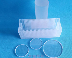
- Surface: DSP, SSP, DSL
- Material: UV Fused Silica, Fused Quartz (JGS1, JGS2, JGS3)
- Primary Flat: 22mm, 32.5mm, 42.5mm, 57.5mm/notch, notch, notch
- Thickness: 350um, 500um, 1000um
- Transmission: Ultraviolet And Visible
Our Fused Silica Wafer product is made of silicon dioxide and is also known as a Silica Crystal Wafer. It is available in different surfaces such as DSP, SSP, and DSL. The material used to make this wafer is UV Fused Silica or Fused Quartz (JGS1, JGS2, JGS3). The wafer has a primary flat of 22mm, 32.5mm, 42.5mm, 57.5mm/notch, notch, or notch. It is available in different thicknesses of 350um, 500um, and 1000um. This wafer has high transmission for ultraviolet and visible light.
Technical Parameters:
| Attribute | Value |
|---|---|
| Product Category | Fused Silica Wafer |
| Diameter | 50.8mm, 76.2mm, 100mm, 150mm, 200mm |
| Bow | ±20µm, ±25µm, ±40µm, ±40µm, ±60µm, ±60µm |
| Thickness | 350um, 500um, 1000um |
| Edge Rounding | Compliant with SEMI M1.2 Standard/refer to IEC62276 |
| Polished side Ra | <1.0nm or specific per requested |
| Primary Flat | 22mm, 32.5mm, 42.5mm, 57.5mm/notch, notch, notch |
| TTV | <8µm, <10µm, <15µm, <20µm, <30µm, <30µm |
| LTV (5mmx5mm) | <2µm |
| Surface | DSP, SSP, DSL |
These technical parameters are for Fused Silica Wafer, also known as Silica Crystal Wafer, Quartz Wafer, or Vitreous Silica Wafer.
Applications:
The Fused Silica Wafer is available in different models, including Fused Silica and Fused Quartz, with a bow ranging from ±20µm to ±60µm. The product is certified by ISO:9001 and ISO:14001, ensuring its high quality. The product is made in China, with a minimum order quantity of 5 pcs. The price is negotiable, with payment terms of T/T.
The Fused Silica Wafer has a supply ability of 20000 pcs/Month, with a delivery time of 1-4 weeks. The product is packaged in cassette/jar package, vacuum-sealed, ensuring its safety and quality.
The Fused Silica Wafer is ideal for various occasions and scenarios, including:
- Semiconductor Fabrication: The Fused Silica Wafer is widely used in semiconductor fabrication, including photolithography, etching, deposition, and bonding. The product's superior optical clarity and chemical stability make it an ideal choice for semiconductor applications.
- MEMS Fabrication: The Fused Silica Wafer is also used in MEMS fabrication, including micro-machining, microfluidics, and biosensors. The product's high-quality material and precise bow make it an ideal choice for MEMS applications.
Overall, the Fused Silica Wafer is a high-quality product that provides superior optical clarity and chemical stability. Its various models and precise bow make it an ideal choice for various semiconductor and MEMS applications.
Support and Services:
Our Fused Silica Wafers are made of high-purity synthetic amorphous silicon dioxide. They have excellent optical, mechanical, and thermal properties, making them ideal for use in a variety of industries such as semiconductors, optics, and electronics.
We provide technical support to help our customers with the selection, customization, and usage of our Fused Silica Wafers. Our team of experts can also assist with any troubleshooting or product-related issues that may arise.
In addition, we offer various services to ensure the highest quality and performance of our Fused Silica Wafers. These include cleaning, polishing, and coating services.
Packing and Shipping:
Our Fused Silica Wafer product is carefully packaged to ensure safe delivery. Each wafer is individually wrapped in a protective film and then placed in a sturdy, foam-lined box to prevent any damage during shipping.
We offer several shipping options to meet your needs, including standard and expedited shipping. Orders are typically processed within 1-2 business days and shipping times vary depending on your location and selected shipping method.
FAQ:
Q1: What is the brand name of the fused silica wafer?
A1: The brand name of the fused silica wafer is BonTek.
Q2: What are the model numbers for the fused silica wafer?
A2: The fused silica wafer is available in two model numbers - Fused Silica and Fused Quartz.
Q3: What certifications does the product have?
A3: The product is certified with ISO:9001 and ISO:14001 certifications.
Q4: What is the minimum order quantity for the fused silica wafer?
A4: The minimum order quantity for the fused silica wafer is 5 pieces.
Q5: What are the packaging details for the fused silica wafer?
A5: The fused silica wafer is packaged in either cassette or jar package and is vacuum sealed for protection during shipping.
Q6: What is the price of the fused silica wafer?
A6: The price of the fused silica wafer is negotiable and will depend on the quantity ordered.
Q7: What are the payment terms for the fused silica wafer?
A7: The payment terms for the fused silica wafer is T/T (Telegraphic Transfer).
Q8: What is the supply ability per month for the fused silica wafer?
A8: The supply ability per month for the fused silica wafer is 20,000 pieces.
Q9: What is the delivery time for the fused silica wafer?
A9: The delivery time for the fused silica wafer is between 1-4 weeks, depending on the quantity ordered and the shipping destination.
![]()
![]()
![]()
![]()
![]()
![]()