


 |
SSP Surface Fused Silica Wafer for MEMS Manufacturing Process
Product Details:
| Place of Origin: | China |
| Brand Name: | BonTek |
| Certification: | ISO:9001, ISO:14001 |
| Model Number: | Fused Silica, Fused Quartz |
Payment & Shipping Terms:
| Minimum Order Quantity: | 5 pcs |
|---|---|
| Price: | Negotiable |
| Packaging Details: | Cassette/ Jar package, vaccum sealed |
| Delivery Time: | 1-4 weeks |
| Payment Terms: | T/T |
| Supply Ability: | 20000 pcs/Month |
|
Detail Information |
|||
| Transmission: | Ultraviolet And Visible | Edge Rounding: | Compliant With SEMI M1.2 Standard/refer To IEC62276 |
|---|---|---|---|
| TTV: | <8µm, <10µm, <15µm, <20µm, <30µm, <30µm | Warp: | <30µm, <40µm, <50µm, <50µm, <60µm, <60µm |
| Material: | UV Fused Silica, Fused Quartz (JGS1, JGS2, JGS3) | Surface: | DSP, SSP, DSL |
| PLTV(<0.5um): | ≥95%(5mm*5mm) | Type: | Fused Silica, Fused Quartz |
| Highlight: | MEMS Manufacturing Process Silica Wafer,SSP Surface Fused Silica Wafer,MEMS Manufacturing Process Fused Silica Wafer |
||
Product Description
Product Description:
Our Fused Silica Wafer is polished to a surface roughness of less than 1.0nm, or can be specified to meet your exact requirements. This level of precision ensures optimal performance in your semiconductor and MEMS applications. Additionally, our wafer meets the edge rounding requirements of the SEMI M1.2 standard, as well as the IEC62276 specification.
We understand that warping can be a concern in many applications, which is why we offer a range of options to suit your needs. Our Fused Silica Wafer is available in warp levels of less than 30µm, less than 40µm, less than 50µm, less than 60µm, and less than 70µm. This allows you to select the level of warping that is most appropriate for your application.
To further ensure the quality of our Fused Silica Wafer, we also measure TTV (total thickness variation) to ensure that it meets your specifications. Our wafer is available with TTV levels of less than 8µm, less than 10µm, less than 15µm, less than 20µm, less than 30µm, and less than 40µm.
Overall, our Fused Silica Wafer is an excellent choice for your semiconductor and MEMS applications. Its exceptional thermal and mechanical properties, combined with its precision polishing and edge rounding, make it a reliable and high-performance option. Choose from our range of warping and TTV options to ensure that our wafer meets your exact specifications.
Features:
- Product Name: Fused Silica Wafer
- Warp: <30µm, <40µm, <50µm, <50µm, <60µm, <60µm
- Product Category: Fused Silica Wafer
-
Material:
- UV Fused Silica
- Fused Quartz (JGS1, JGS2, JGS3)
- Brand: JGS1 JGS2 JGS3
-
Type:
- Fused Silica
- Fused Quartz
Keywords: Crystalline Silica Wafer, Silica Glass Wafer, Fused Quartz Wafer
Technical Parameters:
| Attribute | Options |
|---|---|
| Primary Flat | 22mm, 32.5mm, 42.5mm, 57.5mm/notch, notch, notch |
| TTV | <8µm, <10µm, <15µm, <20µm, <30µm, <30µm |
| Material | UV Fused Silica, Fused Quartz (JGS1, JGS2, JGS3) |
| Edge Rounding | Compliant with SEMI M1.2 Standard/refer to IEC62276 |
| Thickness | 350um, 500um, 1000um |
| Transmission | Ultraviolet And Visible |
| PLTV(<0.5um) | ≥95%(5mm*5mm) |
| Bow | ±20µm, ±25µm, ±40µm, ±40µm, ±60µm, ±60µm |
| Diameter | 50.8mm,76.2mm, 100mm, 150mm, 200mm |
| Polished side Ra | <1.0nm or specific per requested |
This table shows the technical parameters for the Vitreous Silica Wafer product. Other common names for this product include Silica Crystal Wafer and Amorphous Silica Wafer.
Applications:
The Fused Silica Wafer has various models, including JGS1, JGS2, and JGS3, and is suitable for multiple product application occasions and scenarios, such as:
- Optical Products: The Fused Silica Wafer is perfect for superior optical clarity, making it suitable for optical products such as lenses, mirrors, and prisms.
- Semiconductor Industry: The wafer's TTV and Bow attributes make it an ideal product for the semiconductor industry, where precision and uniformity are crucial.
- Research and Development: The Fused Silica Wafer is also suitable for research and development purposes, such as in the fields of nanotechnology and material science.
The Fused Silica Wafer comes with edge rounding compliant with SEMI M1.2 Standard/refer to IEC62276, ensuring a smooth and safe handling experience. The TTV ranges from <8µm to <30µm, while the Bow ranges from ±20µm to ±60µm, depending on the model chosen.
Support and Services:
Our Fused Silica Wafer product comes with comprehensive technical support and services to ensure optimal performance and customer satisfaction. Our team of experts is available to assist with installation, operation, and maintenance of the product, as well as troubleshooting any issues that may arise. Additionally, we offer customized solutions to meet specific customer requirements and provide training to ensure proper usage of the product. Our commitment to quality extends beyond the initial sale, as we offer ongoing support to address any questions or concerns that may arise during the product’s lifespan.
Packing and Shipping:
Product Packaging:
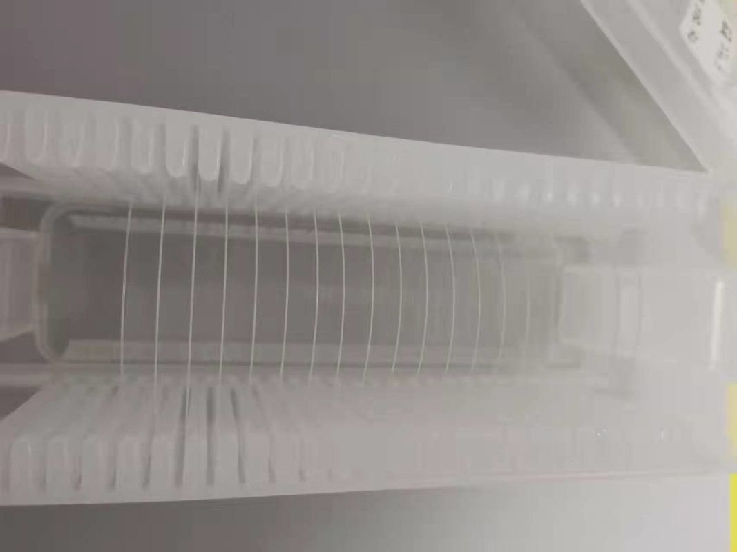
The Fused Silica Wafer product will be packaged securely in a cleanroom environment to prevent any contamination. The wafers will be placed in a wafer carrier with protective foam inserts to prevent any damage during shipping.
Shipping:
The Fused Silica Wafer product will be shipped via a reliable courier service. The package will be marked as fragile and handled with care. The shipping cost will be calculated based on the destination and weight of the package.
FAQ:
Q1: What is the brand name of the product?
A1: The brand name of the product is BonTek.
Q2: What is the minimum order quantity for the Fused Silica Wafer?
A2: The minimum order quantity for the Fused Silica Wafer is 5 pcs.
Q3: What certifications does the product have?
A3: The Fused Silica Wafer is certified with ISO:9001 and ISO:14001.
Q4: What is the packaging method for the Fused Silica Wafer?
A4: The Fused Silica Wafer is packaged in either a cassette or jar package and is vacuum sealed.
Q5: What is the delivery time for the Fused Silica Wafer?
A5: The delivery time for the Fused Silica Wafer is 1-4 weeks.
![]()
![]()
![]()
![]()
![]()
![]()