

 |
Sapphire Al2O3 Crystal Substrate Ultrathin 2" 3"Double Side Polished For Optical
Product Details:
| Place of Origin: | China |
| Brand Name: | CSIMC |
| Certification: | ISO:9001 |
| Model Number: | Sapphire (Al2O3) |
Payment & Shipping Terms:
| Minimum Order Quantity: | 5 Pieces |
|---|---|
| Price: | Negotiable |
| Packaging Details: | Cassette, Jar, Film package |
| Delivery Time: | 1-4 weeks |
| Payment Terms: | T/T |
| Supply Ability: | 10000 pieces/Month |
|
Detail Information |
|||
| Material Name: | Sapphire (Al2O3) Crystal | Type: | Single Crystal |
|---|---|---|---|
| Size: | 2" | Purity: | 99.999% |
| Surface Finish: | DSP/SSP | VIS Range: | 85% |
| Application: | Semicondutor Wafer, Led Chip, Optical Glass Window, Electronic Ceramics | Industry: | Led,optical Glass,eli-ready Wafer |
| Highlight: | Double Side Polished Sapphire Crystal Substrate,Optical Sapphire Crystal Substrate,Ultrathin Sapphire Crystal Substrate |
||
Product Description
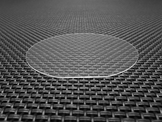
Sapphire Al2O3 Crystal Substrate Ultrathin 2" 3"Double Side Polished For Optical
Discover the high-quality of Sapphire crystal wafers. These high-quality wafers are precision-cut from genuine Sapphire crystal, offering unparalleled durability and exceptional optical properties. Ideal for a range of applications including optics, sensors, and high-end jewelry, Sapphire crystal wafers are the perfect choice for those who demand the ultimate in quality and performance. With their unique properties and stunning appearance, Sapphire crystal wafers are sure to make a statement in any application.
![]()
![]()
![]()
![]()
The main specifications for sapphire crystal substrates
|
|
Unit |
Specification |
||
|
2 Inch Substrate |
4Inch Substrate |
6 Inch Substrate |
||
| Diameter | mm | 50.8±0.1 | 100±0.1 | 150±0.2 |
| Thickness | um | 430±10 | 650±10 | 1300±20 |
| Surface Orientation of A-plane | Degree | 0°±0.1° | 0°±0.1° | 0°±0.1° |
| Surface Orientation of M-plane | Degree | 0.2°±0.05° | 0.2'±0.05° | 0.2°±0.05 |
| Primary Flat Length | mm | 16±1.0 | 30±1 | 47.5±1 or 25±1 |
| Primary Flat Orientation | Degree | A-plane±0.25° |
A-plane±0.25° |
A-plane±0.25° |
| Back Side Roughness | um | 1.0±0.2 | 1.0±0.2 | 1.0±0.2 |
| Front Side Roughness | nm | ≤0.2 | ≤0.2 | ≤0.2 |
| Wafer Edge | Type | R or T | R or T | T |
| Total Thickness Variation,TTV | um | ≤6 | ≤6 | ≤10 |
| SORI | um | ≤15 | ≤15 | ≤15 |
| BOW | um | -10~0 | -10~0 | -10~0 |
![]()
Want to Know more details about this product