

 |
Diameter 2-12 Inch Silica Wafer With TTV 5um Glass Substrates
Product Details:
| Place of Origin: | China |
| Brand Name: | BonTek |
| Certification: | ISO:9001 |
| Model Number: | Glass substrates |
Payment & Shipping Terms:
| Minimum Order Quantity: | 5 pcs |
|---|---|
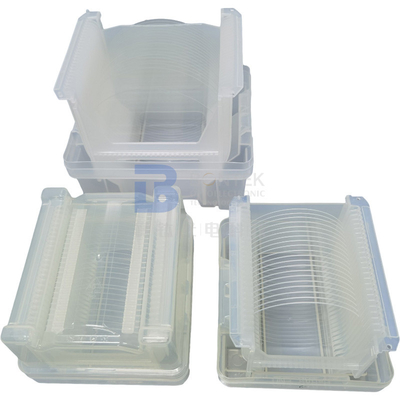
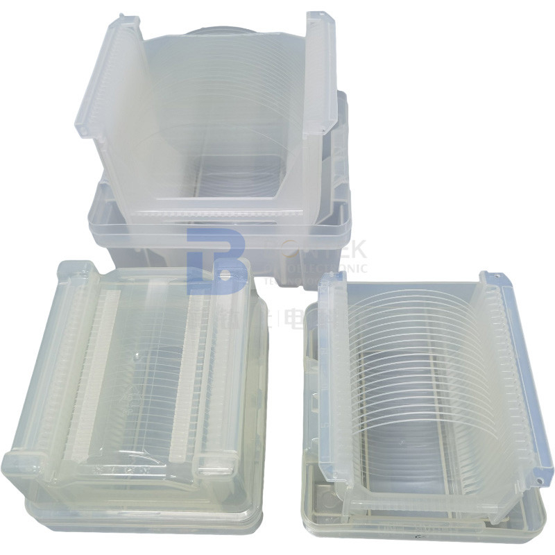
| Packaging Details: | Cassette, Jar |
| Delivery Time: | 2 weeks |
| Payment Terms: | TT/in advance |
| Supply Ability: | 100000/month |
|
Detail Information |
|||
| Damage Threshold: | >10J/cm2 | Reflectance: | <0.25% |
|---|---|---|---|
| Parallelism: | 3 Arc Sec | BOW: | <30um |
| Transmission: | IR, Visible, DUV | Inspection Report: | Per Request |
| FLH Model: | JGS1, JGS2, JGS3, F-HUV | Material: | Fused Silica Glass |
| Highlight: | 12 Inch Silica Wafer,fused quartz wafers with TTV,5um Glass Substrates Silica Wafer |
||
Product Description
Product Description:
Fused Silica Wafer is an optical-grade monocrystalline wafer made of quartz material, also known as fused quartz or fused silica. It has excellent optical properties, such as transmission range from 0.17 to 2.1um, 0.26 to 2.1um and 0.0185 to 3.5um, warp less than 35um, FLH Models such as JGS1, JGS2, JGS3 and F-HUV, second flat per request, and surface roughness Ra less than 1.0nm. In comparison with other materials such as calcium silicate board and borosilicate glass, it has higher optical transmission, less thermal expansion coefficient, and better homogeneity. Fused Silica Wafer is the ideal material for high-precision optical components, such as lenses, windows, and prisms.
Features:
- Product Name: Fused Silica Wafer
- Transmission: IR, Visible, DUV
- Metal Impurities: <0.2ppm
- BOW: <30um
- TTV: <2um, <5um
- Material: Fused Silica Glass
- Glass Wafer
- Fused Quartz Labware
- Aluminum Silicate Glass
- Optical Glass
Technical Parameters:
| Material | UV Fused Silica, Fused Quartz (JGS1, JGS2, JGS3) | ||||||
| Specification | unit | 3” | 4” | 5" | 6" | 8" | 12" |
| Diameter (or Square) | mm | 76.2 | 100 | 125 | 150 | 200 | 300 |
| Tol(±) | mm | <0.1~0.25 mm | |||||
| Thinnest Thickness | mm | >0.10 | >0.10 | >0.30 | >0.30 | >0.30 | >0.50 |
| Primary Flat | mm | 22 | 32.5 | 42.5 | 57.5/notch | notch | notch |
| LTV (5mmx5mm) | µm | <2 | <2 | <2 | <2 | <2 | <10 |
| TTV | µm | <8 | <10 | <15 | <20 | <30 | <30 |
| Bow | µm | ±20 | ±25 | ±40 | ±40 | ±60 | ±60 |
| Warp | µm | <30 | <40 | <50 | <50 | <60 | <60 |
| PLTV(<0.5um) | % | ≥95%(5mm*5mm) | |||||
| Transmittance | UV, Optical, IR or Custom option | ||||||
| Edge Rounding | mm | Compliant with SEMI M1.2 Standard/refer to IEC62276 | |||||
| Surface Type | Single Side Polished /Double Sides Polished | ||||||
| Polished side Ra | nm | <1.0nm or specific per requested | |||||
| Back Side Criteria | µm | General is 0.2-0.5µm or as customized | |||||
| Appearance | Contamination | None | |||||
| Particles>0.3µm | <=30 | ||||||
| Saw Marks, striations | None | ||||||
| Scratch | None | ||||||
| Cracks, saw marks, stains | None | ||||||
| Parameters | Specifications |
|---|---|
| Parallelism | 3 Arc Sec |
| Warp | <35um |
| Transmission | IR, Visible, DUV |
| Density | 2.20g/cm3 |
| Certificate | ISO9001, RoHS |
| OH Content | <5ppm, <10ppm, <100ppm |
| Damage Threshold | >10J/cm2 |
| FLH Model | JGS1, JGS2, JGS3, F-HUV |
| Thickness | 0.1-10mm |
| Surface Quality | 20-10 |
| Fused Quartz Labware | High Purity Fused Silica |
| Aluminum Silicate Glass | Yes |
![]()
![]()
Applications:
Customization:
- Brand Name: BonTek
- Model Number: Glass substrates
- Place of Origin: China
- Certification: ISO:9001
- Minimum Order Quantity: 5 pcs
- Packaging Details: Cassette, Jar
- Delivery Time: 2 weeks
- Payment Terms: TT/in advance
- Supply Ability: 100000/month
- Diameter: 2-12 Inch
- Refractive Index: 1.46, 1.472, 1.50, 1.51, 1.523
- Transmission Range: 0.17~2.1um, 0.26~2.1um, .0185~3.5um
- Warp: <35um
- FLH Model: JGS1, JGS2, JGS3, F-HUV
- Keywords: Calcium Silicate Board, alumina silicate glass, Calcium Silicate Board, high-temperature insulation material
Support and Services:
We provide technical support and service for Fused Silica Wafer. Our experienced technicians and engineers can provide the following services:
- Repair and maintenance of Fused Silica Wafer products
- Consulting and troubleshooting of Fused Silica Wafer issues
- Installation and configuration of Fused Silica Wafer
- Testing and evaluation of Fused Silica Wafer
- Software upgrades for Fused Silica Wafer
- Training and support for Fused Silica Wafer
If you have any questions or need support for your Fused Silica Wafer, please contact us for more information.