


|
Unlocking Lithium Tantalate On Insulator ( LTOI ) For Advanced Photonic Applications
Product Details:
| Place of Origin: | China |
| Brand Name: | BonTek |
| Certification: | ISO:9001, ISO:14001 |
| Model Number: | LNOI Wafer |
Payment & Shipping Terms:
| Minimum Order Quantity: | 25 pcs |
|---|---|
| Price: | $2000/pc |
| Packaging Details: | Cassette/ Jar package, vaccum sealed |
| Delivery Time: | 1-4 weeks |
| Payment Terms: | T/T |
| Supply Ability: | 50000 pcs/Month |
|
Detail Information |
|||
| Product: | LiTaO3 On Insulator | Diameter: | 4 Inch, Φ100mm |
|---|---|---|---|
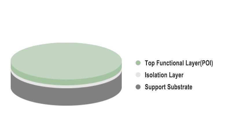
| Top Layer: | Lithium Tantalate | Top Thickness: | 300~600nm |
| Insolation: | SiO2 Thermal Oxide | Insolation Thickness: | 2000±15nm; 3000±50nm; 4700±100nm |
| Substrate: | Silicon Wafer | Application: | Optical Waveguides And Microwaveguides |
| Highlight: | Photonic Lithium Tantalate On Insulator,LTOI Piezoelectric Wafer |
||
Product Description
Unlocking the Potential of Lithium Tantalate on Insulator (LTOI) for Advanced Photonic Applications
LTOI stands for Lithium Tantalate on Insulator, is a specialized substrate technology used in the field of integrated photonics. It involves the transfer of a thin layer of lithium tantalate (LiTaO3) crystal onto an insulating substrate, typically silicon dioxide (SiO2) or silicon nitride (Si3N4). LTOI substrates offer unique advantages for the development of compact and high-performance photonic devices.
LTOI substrates are created through a bonding process where a thin layer of lithium tantalate crystal is transferred onto an insulating substrate. This process can be achieved through various techniques, including wafer bonding or ion-cutting, ensuring a strong bond between the layers.
LTOI substrates offer unique advantages for advanced photonic applications. Their utilization in electro-optic modulators, waveguides, nonlinear optical devices, sensors, quantum photonics, and integrated photonic circuits demonstrates the broad range of applications and the potential for pushing the boundaries of integrated photonics technology.
| LTOI Wafer | |||
| Structure | LiTaO3 / SiO2 / Si | LTV / PLTV | < 1.5 μm ( 5∗ 5 mm2 ) / 95% |
| Diameter | Φ100 ± 0.2 mm | Edge Exclution | 5 mm |
| Thickness | 500 ± 20 μm | Bow | Within 50 μm |
| Primary Flat Length | 47.5 ± 2 mm 57.5 ± 2 mm |
Edge Trimming | 2 ± 0.5 mm |
| Wafer Beveling | R Type | Environmental | Rohs 2.0 |
| Top LT Layer | |||
| Average Thickness | 400/600±10 nm | Uniformity | < 40nm @17 Points |
| Refraction index | no > 2.2800, ne < 2.2100 @ 633 nm | Orientation | Z axis ± 0.3° |
| Grade | Optical | Surface Ra | < 0.5 nm |
| Defects | >1mm None; ≦1 mm Within 300 total |
Delamination | None |
| Scratch | >1cm None; ≦1cm Within 3 |
Primary Flat | Perpendicular to +Y Axis ± 1° |
| Isolation SiO2 Layer | |||
| Average Thickness | 2000nm ± 15nm 3000nm ± 50nm 4700nm ± 100nm | Uniformity | < ±1% @17 Points |
| Fab. Method | Thermal Oxide | Refraction index | 1.45-1.47 @ 633 nm |
| Substrate | |||
| Material | Si | Orientation | <100> ± 1° |
| Primary Flat Orientation | <110> ± 1° | Resistivity | > 10 kΩ·cm |
| Backside Contamination | No visible stain | Backside | Etch |
![]()
![]()
![]()
![]()