


 |
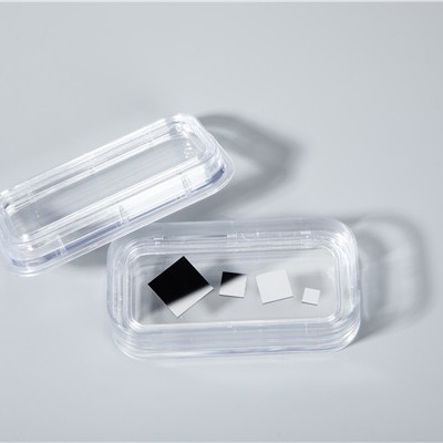
Single Side Polished Square SrTiO3 Crystal Wafer 10mm For Semiconductor
Product Details:
| Place of Origin: | China |
| Brand Name: | BonTek |
| Certification: | ISO:9001, ISO:14001 |
| Model Number: | SrTiO3 crystal |
Payment & Shipping Terms:
| Minimum Order Quantity: | 10 pcs |
|---|---|
| Price: | Negotiable |
| Packaging Details: | Cassette/ Jar package, vaccum sealed |
| Delivery Time: | 1-4 weeks |
| Payment Terms: | T/T |
| Supply Ability: | 50000 pcs/Month |
|
Detail Information |
|||
| Material: | SrTiO3 Single Crystal | Orientation: | <100>、<110>、<111>±0.5o |
|---|---|---|---|
| Crystal Structure: | Cubic System (a=3.905Å) | Density: | 5.175g/cm3 |
| Surface: | Single Side Polished | CTE: | 10.4 Ppm/℃ |
| Growth Method: | Flame Method | Dielectric Constant: | 9.8 |
| Highlight: | Single Side Polished SrTiO3 Crystal Wafer,SrTiO3 Crystal Wafer 10mm,Semiconductor SrTiO3 Single Crystal |
||
Product Description
10mm Square SrTiO3 Crystal Wafer For Semiconductor
SrTiO3 single crystal has the good lattice structure of perovskite structure materials. For the epitaxial growth of HTS and most oxide films, SrTiO3 single crystal is an excellent substrate material. It has been widely used in the study of high temperature superconducting thin films, and also widely used in special optical Windows and high quality sputtering targets.
![]()
![]()
![]()
| SrTiO3 Crystal | |
| Crystal structure | Cubic system (a=3.905Å) |
| Density | 5.175g/cm3 |
| Dopant | Intrinsic, Fe doped, neodymium (Nd) doped, Niobium doped |
| Coefficient of thermal expansion | 10.4ppm/℃ |
| Dielectric constant | 9.8 |
| Orientation | <100>,<110>,<111>±0.5o,as required |
| Dimension | Dia30×0.5mm, 20×20×0.5mm, 15×15×0.5mm 10×10×0.5mm, 10×5×0.5mm, 5×5×0.5mm |
| Surface Finish | 单面或双面抛光 |
| Surface Roughness | ≤5Å |
| Package | 100 Class Clean Bag, Jar package, Film package
|
![]()
![]()
Want to Know more details about this product